Objectives
The ultimate goal of the project is to design a circuit that meets certain design requirements.
Tools
- Lab Equipment
- Circuit Simulator
- Hantek 3-in-1 Digital Equipment
- Powered Breadboard
Assessment
The overall weighted grading scheme is as follows:
Table 1 Overall Weighted Grading Scheme
| Category | Percent of Overall Grade |
|---|---|
| Circuit Design | 45% |
| Demo | 15% |
| Report | 40% |
| Total | 100% |
I. Circuit Design and Demo
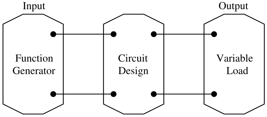
Figure 1 Single-Input Single-Output (SISO) System
Figure 1 shows a single-input single-output (SISO) system considered in this project. In the system, a function generator acts as the input while the output is a variable load. As shown in Figure 2, the function generator can be modeled by an independent voltage source connected in series with a resistor while the variable load is modeled using a resistor with variable resistance.
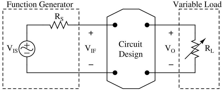
Figure 2 Circuit Model
Each of the five notations used in Figure 2 represents a physical quantity. The representations are described in the following list.
VIS − input signal voltage
VIF − input voltage to the designed circuit
VO − output voltage
RS − output impedance of a function generator with a typical value of 50Ω
RL − variable load with resistance in the range of R_{MIN} \le R_L \le R_{MAX}
In this project, your group has been tasked by Chanos to design a circuit that meets certain design requirements and specifications. The tasks required to be completed are as follows:
- Design ONE circuit that will satisfy all the design specifications detailed in Table 2.
- The ONE circuit that you design must work for the entire range of RL specified in Table 2.
- Demonstrate both simulation and experimental results of your designed circuit on the spot to your Lab TA. Provide detailed explanations and reasonings on how you have obtained the results during your demo.
- Record down your results for the writing of your report.
The following table contains the set of specifications that your designed circuit has to meet.
Table 2 Design Specifications
| Lab Section | Design Specification |
|---|---|
| EEL 3123C-11 | Project A |
| EEL 3123C-12 | Project C |
| EEL 3123C-13 | Project D |
| EEL 3123C-14 | Project E |
| EEL 3123C-15 | Project F |
| EEL 3123C-16 | Project B |
The grades earned in this part depend highly on your ability to complete the above tasks. The weighted grading scheme is as follows:
Table 3 Weighted Grading Scheme for Circuit Design and Demo
| Category | Percent of Overall Grade |
|---|---|
| Simulation Results and Achievement | 10% |
| Experimental Results and Achievement | 35% |
| Simulation Demonstration and Elaboration | 5% |
| Experimental Demonstration and Elaboration | 10% |
| Total | 60% |
IMPORTANT NOTES:
- DO NOT blindly play around with component values using a circuit simulator in the hope that you will discover a working design. Even if you somehow manage to discover a working design magically, you will still lose substantial points in this project since you won’t be able to dissect your circuit design in your report using circuit theory, calculations, etc.
- Collaborations between any groups are strictly prohibited in this project.
- All project demonstrations must be performed during a lab session. No project demonstration can be performed outside lab session.
- All groups will be given only ONE lab session to demonstrate a working design on the spot.
- HEADS UP: It is impossible to complete all the required tasks in this project in a 2-hour lab session. To prepare fully for your project execution and demonstration, you are highly encouraged to perform circuit simulations and experiments at home so that you can figure out a working design for your project. To perform experiments outside of the laboratory, you can loan out a Hantek 3-in-1 digital equipment and a powered breadboard. You can also acquire circuit components from the laboratory, and they are not required to be returned.
- SUGGESTION: You are strongly encouraged to complete the following tasks prior to your lab session.
- Perform all simulation work.
- Build, test and verify the functionality of your designed circuit using the Hantek 3-in-1 digital equipment and powered breadboard you have loaned out.
If you have completed all of the above tasks in advance, all you have to do during your lab session is to connect the instruments in the laboratory to the constructed circuit on the loaned breadboard and perform your demo. In this case, you can literally walk out of your lab session with a great sense of accomplishment in 30 minutes.
TECHNICAL NOTES:
- The use of op-amp is strictly prohibited in this project.
- If you use an inductor, you ought to measure its resistance using a DMM. Record down the measured value and incorporate this non-ideal factor, specifically the DC resistance (DCR) value of an inductor into your analysis. Welcome to the real world!
II. Report
Document all your analysis, results and findings in a report. The content of your report should include, but not limited to, the following sections.
- Objectives and Tasks – define and outline explicitly the objectives and tasks
- Dissection of Design – present your circuit design in a detailed, part-by-part analysis
– explain the reasonings behind your circuit design using circuit theory– provide detailed circuit analysis and calculation to justify the circuit topology,component type and component value used in your design
- Simulation Results – present your simulation results with clarity
– include screenshots of simulated circuits, results, etc.
- Experimental Results – present your experimental results with clarity
– include oscilloscope figures, screenshots of DMM measurements, etc.
- Results Comparison – compare simulation and experimental results
– explain discrepancies pertaining to concepts
- Conclusions
The weighted grading scheme is as follows:
Table 4 Weighted Grading Scheme for Report
| Category | Percent of Overall Grade |
|---|---|
| Objectives and Tasks | 2.5% |
| Dissection of Design | 25.0% |
| Simulation Results | 2.5% |
| Experimental Results | 2.5% |
| Results Comparison | 5.0% |
| Conclusions | 2.5% |
| Total | 40% |
IMPORTANT NOTES:
- The dissection of design is a very critical part in your report. You will lose substantial points if you fail to provide detailed circuit analysis and calculation to explain the reasonings behind your circuit design.