In this first part, the goal is to design two circuits that meet certain design requirements under certain design constraints.
Design Requirement
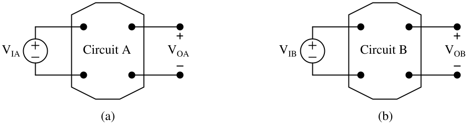
- Referring to Figure 1 (a), design Circuit A such that VOA = KA×VIA, where VIA and VOA are the input and output voltages respectively.
- Referring to Figure 1 (b), design Circuit B such that VOB = KB×VIB, where VIB and VOB are the input and output voltages respectively.
- The values for KA and KB are provided in Table 2.
Table 2 Design Specifications
| Lab Section | Design Specification |
|---|---|
| EEL 3123C-11 | KA = 0.6 and KB = 0.5 |
| EEL 3123C-12 | KA = 0.75 and KB = 0.6 |
| EEL 3123C-13 | KA = 0.5 and KB = 0.9 |
| EEL 3123C-14 | KA = 0.9 and KB = 0.8 |
| EEL 3123C-15 | KA = 0.8 and KB = 0.75 |
| EEL 3123C-16 | KA = 0.8 and KB = 0.9 |
Design Constraint
- You are allowed to use resistors with resistances within the range of 1 kΩ to 10 kΩ only. Refer to APPENDIX II for available resistors.
- Use as FEWEST components as possible.