Objectives
The ultimate goal of the project is to identify the circuit elements used in a given circuit.
Tools
- Lab Equipment
- Circuit Simulator
- Hantek 3-in-1 Digital Equipment
- Powered Breadboard
Assessment
The overall weighted grading scheme is as follows:
Table 1 Overall Weighted Grading Scheme
| Category | Percent of Overall Grade |
|---|---|
| Circuit Element Identification | 50% |
| Demo | 15% |
| Report | 35% |
| Total | 100% |
I. The Challenge
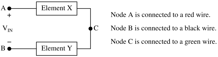
Figure 1 Schematic of Circuit Under Test (CUT)
Figure 1 shows the schematic of the circuit considered in this project. The circuit of interest is named Circuit Under Test (CUT) and has the following characteristics.
- The CUT contains TWO circuit elements only: Element X and Element Y.
- The two circuit elements are connected in series.
- Both Element X and Element Y can be a resistor, inductor or capacitor.
- The CUT must contain at least one resistor. This means that the circuit of interest can be a RR, RL or RC circuit only.
At the start of a lab session, each group will be given a CUT that contains randomly chosen element type and value. With the CUT concealed in a box, your group is tasked with the challenge to achieve the following four objectives by the end of your lab session.
- Identify the type of element that is connected between node A and node C. In other words, determine if Element X is a resistor, inductor or capacitor.
- Determine the value for Element X. The predicted value must fall within of the actual component value.
- Identify the type of element that is connected between node B and node C. In other words, determine if Element Y is a resistor, inductor or capacitor.
- Determine the value for Element Y. The predicted value must fall within of the actual component value.
The grades earned in this first category of assessment depend highly on your success in achieving the four objectives described above. The weighted grading scheme is as follows:
Table 2 Weighted Grading Scheme for Circuit Element Identification
| Category | Percent of Overall Grade |
|---|---|
| Identification of Element Type for Element X | 5% |
| Identification of Element Type for Element Y | 5% |
| Determination of Element Value for Element X | 20% |
| Determination of Element Value for Element Y | 20% |
| Total | 50% |
In the process of working towards the above objectives, you MUST follow the following rules. Violation of any of the following rules will result in penalty detailed in Table 3 below.
- Rule #1: You are NOT allowed to unveil the CUT concealed in a box to help you achieve any of the four objectives described above.
- Rule #2: You are NOT allowed to use the resistance measuring function on any instrument including digital multimeter (DMM), LCR meter, etc. to measure directly the resistance of any circuit element.
- Rule #3: You are NOT allowed to use the capacitance measuring function on any instrument including digital multimeter (DMM), LCR meter, etc. to measure directly the capacitance of any circuit element.
- Rule #4: You are NOT allowed to use the inductance measuring function on any instrument including digital multimeter (DMM), LCR meter, etc. to measure directly the inductance of any circuit element.
- Rule #5: For any input that you apply to the CUT, the input can only be connected between node A and node B. In other words, you are NOT allowed to apply any input between node A and node C as well as between node B and node C.
- You are allowed to take voltage and current measurement at any node.
- You are allowed to connect any circuit element externally to the CUT concealed in a box.
Table 3 Penalty for Rule Violation
| Action | Consequence |
|---|---|
| Violation of Rule #1 | Overall project grade will be ZERO. |
| Violation of Rule #2, #3, #4 or #5 | For each offense, 50% will be deducted from overall project grade. |
IMPORTANT NOTES:
- WARNING: If you unveil the CUT concealed in a box to help you achieve any of the four objectives described above, you will earn a grade of zero for this specific project regardless of how much work you have completed. Penalty for the violation of Rule #1 will be strictly enforced.
- WARNING: Pay attention to all the rules and penalties described above. Please understand that the penalties are not created to destroy your grade; they are established for the sole purpose of ensuring fairness among all students who work on this project.
- Collaborations between any groups are strictly prohibited in this project.
TECHNICAL NOTES:
- WARNING: If you use a DC power supply, be mindful of the current setting on the equipment to avoid undesirable incident.
- Frequency response higher than 500 kHz will not be considered in this project.
II. Demo
Perform the following tasks.
- Provide the element type and value you have predicted for both Element X and Element Y to your Lab TA.
- Demonstrate to your Lab TA how you have arrived at your conclusions. Provide detailed explanations and reasonings on how you have obtained the results during your demo.
- Record down your results for the writing of your report.
The weighted grading scheme for Demo is as follows:
Table 4 Weighted Grading Scheme for Demo
| Category | Percent of Overall Grade |
|---|---|
| Experimental Demonstration and Elaboration | 15% |
| Total | 15% |
IMPORTANT NOTES:
- All project demonstrations must be performed during a lab session. No project demonstration can be performed outside lab session.
- All groups will be given only ONE lab session to demonstrate the accomplishment of the objectives described above.
- HEADS UP: It is impossible to develop a working plan in a 2-hour lab session. To prepare fully for your project execution and demonstration, you are highly encouraged to perform circuit simulations and experiments at home so that you can figure out a plan for your project. To perform experiments outside of the laboratory, you can loan out a Hantek 3-in-1 digital equipment and a powered breadboard. You can also acquire circuit components from the laboratory, and they are not required to be returned.
- SUGGESTION: You are strongly encouraged to complete the following tasks prior to your lab session.
- Establish an experimental plan to identify the type of circuit element. Elimination of possibilities can be a good strategy here.
- Establish an experimental plan to determine the value of circuit element.
III. Report
Document all your analysis, results and findings in a report. The content of your report should include, but not limited to, the following sections.
- Objectives and Tasks – define and outline explicitly the objectives and tasks
- Dissection of Experimental Plan – present your plan in a detailed, part-by-part analysis
– explain the reasonings behind your plan using circuit theory– provide detailed circuit analysis and calculation to justify your plan
- Experimental Results – present your experimental results with clarity
– include oscilloscope figures, screenshots of DMM measurements, etc.
- Results Comparison – compare predicted element type and value with actual element
– analyze failure or success using circuit theory
- Conclusions
The weighted grading scheme is as follows:
Table 5 Weighted Grading Scheme for Report
| Category | Percent of Overall Grade |
|---|---|
| Objectives and Tasks | 2.5% |
| Dissection of Experimental Plan | 15.0% |
| Experimental Results | 5.0% |
| Results Comparison | 10.0% |
| Conclusions | 2.5% |
| Total | 35% |