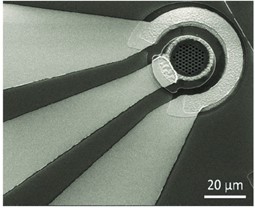
 Quantum Emitter and spin-photon interface in Silicon
Silicon’s scalability and compatibility with mature semiconductor fabrication processes make it an ideal platform for large-scale integration. However, the absence of an efficient spin-photon interface has long limited its role in quantum information science. Our research aims to overcome this barrier by investigating the fundamental properties of silicon-based color centers—emerging quantum emitters with optically addressable spin states. We focus on engineering and integrating these defect centers into nanophotonic and quantum photonic systems to realize coherent spin-photon interfaces within a fully CMOS-compatible platform. By advancing silicon’s quantum capabilities, this work opens pathways toward scalable quantum information processing, quantum communication, and quantum network architectures, leveraging the same material foundation that underpins today’s classical technologies.
Selected Publications
- K. Jhuria, V. Ivanov, D. Polley, Y. Zhiyenbayev, W. Liu, A. Persaud, W. Redjem, W. Qarony, P. Parajuli, Q. Ji, A. J. Gonsalves, J. Bokor, L. Z. Tan, B. Kanté, and T. Schenkel, “Programmable quantum emitter formation in silicon”, Nature Communications, vol. 15, p. 4497, May2024
- W. Redjem#, Y. Zhiyenbayev#, W. Qarony#, V. Ivanov, C. Papapanos, W. Liu, K. Jhuria, Z. Y. Al Balushi, S. Dhuey, A. Schwartzberg, L. Z. Tan, T. Schenkel, and B. Kanté, “All-silicon quantum light source by embedding an atomic emissive center in a nanophotonic cavity”, Nature Communications, vol. 14, p. 3321, Jun 2023
- W. Qarony, W. Redjem, Y. zhiyenbayev, S. Ivanov, C. Papapanos, W. Liu, S. Dhuey, A. Schwartzberg, T. Schenkel, L. Z. Tan, B. Kanté, ” All-silicon quantum light source by embedding a single color center in a nanophotonic cavity“, IEEE Photonics Conference (IPC) (2023).
- Z. Jia, W. Qarony, J. Park, S. Hooten, D. Wen, Y. Zhiyenbayev, W. Redjem, E. Yablonovitch, B. Kanté*, “Interpretable inverse-designed cavity for on-chip nonlinear and quantum optics,” Optica 10(11), 1529-1534(2023).
- R. Contractor#, W. Noh#, W. Redjem#, W. Qarony, E. Martin, S. Dhuey, A. Schwartzberg, B. Kanté*, “Scalable single-mode surface emitting laser via open-Dirac singularities,” Nature 608, 692–698 (2022).
- Y. zhiyenbayev, W. Redjem, S. Ivanov, W. Qarony, W. Liu, C. Papapanos, T. Schenkel, L. Z. Tan, B. Kanté*, “Scalable manufacturing of quantum emitters in silicon by rapid thermal annealing,”
Optics Express 31 (5), 8352-8362 (2023).
 Nanophotonic-based single-photon quantum sensors
Conventional silicon photomultipliers (SiPMs) have long been foundational to photon detection technologies. However, their performance is inherently limited by material properties and device architectures, particularly in terms of photodetection efficiency, timing resolution, and operation at elevated temperatures. Our research addresses these limitations by developing nanophotonic-enhanced single-photon detectors that deliver high-performance operation in demanding environments. By integrating advanced nanophotonic structures with engineered silicon-on-insulator (SOI) platforms, ultrawide bandgap semiconductors, and high-temperature superconductors, we are creating a new generation of quantum sensors with unprecedented capabilities. These detectors are designed for a wide range of applications, including on-chip quantum sensing for scalable quantum networks and quantum computing, medical imaging, semiconductor diagnostics, and optical sensing in extreme environments—from deep-space exploration to high-temperature industrial settings. Our ultimate goal is to advance the frontiers of single-photon and quantum-level detection, enabling transformative breakthroughs in next-generation photonic and quantum technologies.
Selected Publications
- W. Qarony, A. S. Mayet, E. Ponizovskaya-Devine, S. Ghandiparsi, C. Bartolo-Perez, A. Ahamed, A. Rawat, H. H. Mamtaz, T. Yamada, S.-Y. Wang, and M. S. Islam, “Achieving higher photoabsorption than group III-V semiconductors in ultrafast thin silicon photodetectors with integrated photon-trapping surface structures”, Advanced Photonics Nexus, vol. 2, no. 5, p. 056001, 2023
- C. Bartolo-Perez, W. Qarony, S. Ghandiparsi, A.S. Mayet, A. Ahamed, H. Cansizoglu, Y. Gao, E.P. Devine, T. Yamada, A.F. Elrefaie, S.-Y. Wang, M.S. Islam*, “Maximizing Absorption in Photon-Trapping Ultrafast Silicon Photodetectors“, Adv. Photonics Res. 2, 2000190, 2021.
- C. Bartolo-Perez, S. Chandiparsi, A. S. Mayet, H. Cansizoglu, Y. Gao, W. Qarony, A. AhAmed, S.-Y. Wang, S. R. Cherry, M. S. Islam, and G. A. Estrada, “Avalanche photodetectors with photon trapping structures for biomedical imaging applications”, Opt. Express, vol. 29, pp. 19024–19033, Jun 2021
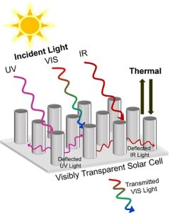 Photonic nanostructure for integrated ubiquitous energy
Photonic nanostructures—such as integrated nanoantennas—offer powerful control over light–matter interactions and enable precise tuning of photon absorption in semiconductors. Our research focuses on the design, material integration, and nanofabrication of such structures to realize visibly transparent, high-efficiency solar cells. By leveraging advanced photonic engineering, we aim to develop solar technologies that can be seamlessly embedded into everyday surfaces and devices. These transparent solar cells are ideally suited for smart windows, agrivoltaic systems in both open-field and greenhouse cultivation, and energy-autonomous mobile electronics and appliances—all without compromising aesthetics or functionality. Our vision is to create ubiquitous, integrated energy-harvesting solutions that merge sustainability with seamless user experience, supporting the global transition to clean and distributed energy systems.
Selected Publications
- W. Qarony, M. I. Hossain, A. Tamang, V. Jovanov, M. Shahiduzzaman, M. S. Ahamed, R. A. Pala, A. Salleo, Y. H. Tsang, and D. Knipp, “On the potential of optical nanoantennas for visibly transparent solar cells”, ACS Photonics, vol. 10, no. 12, pp. 4205–4214, 2023